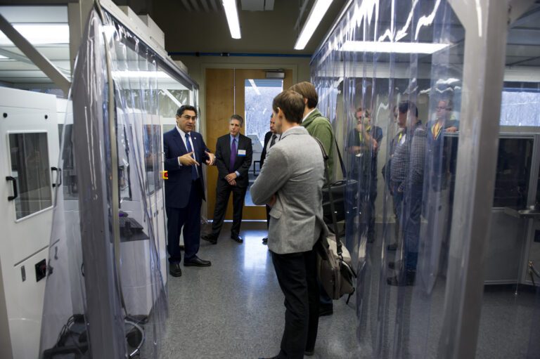
$3 Million Grant Creates Advanced Nanomanufacturing Cluster for Smart Centers and Materials (CSSM)
The Massachusetts Technology Partnership Collaborative Research and Development Grant Program has awarded a $3 million grant to Northeastern to create the Advanced Nanomanufacturing Cluster for Smart Sensors and Materials, or CSSM, which includes research universities and private manufacturing companies.
Advanced nanotechnology has enormous potential to advance connected technologies, known as the Internet of Things, and revolutionize the sensing industry. This includes potential commercial applications such as tiny, high-precision wireless sensors used to monitor premature babies in hospital neonatal units, wearable health and fitness sensors that monitor biomarkers such as glucose, lactate or other biometrics, and sensors that monitor water quality .
The initiative will leverage Northeastern's innovative Nanoscale Offset Printing System, or NanoOPS, a manufacturing technology pioneered by the College's NSF Center for High-Throughput Nanotechnology (CHN), led by University Distinguished Professor Ahmed Busnaina and the William Lincoln Smith Chair in College of Engineering. NanoOPS can print nanoscale sensors and devices as small as 20 nanometers—more than 10,000 times thinner than a human hair—on various surfaces and 100 to 1,000 times faster than current electronic and inkjet-based 3D printing.
Part of the new funding will be used to build infrastructure to characterize materials and test smart sensor prototypes, and to build generation 2 and 3 NanoOPS with enhanced capabilities at the institute, including the ability to print on any surface. The grant is matched by nearly $11 million in external funding through this collaboration between academia, industry and government.
In cooperation with:
Chesterton, DIC Corporation, DRAPER, CABLE, GE, MOXTEK, NASA, Northrop Grumman, Raytheon, Renesas Electronic, Milara, NBMC, Rogers Corporation, Tufts University, University of Massachusetts Boston and US Air Force.
Suggested Cluster Activities
- Design, develop and manufacture product prototypes based on technologies using smart sensors and advanced materials.
- Improvement of physical infrastructure, including purchase of instruments and equipment for material characterization and product testing
- Design and manufacture of 2nd generation NanoOPS that was capable of printing on any substrate.
- Workforce development, such as seminars and workforce training programs to introduce and expose a highly educated workforce currently out of the labor market.
- Study advanced materials and product lifecycle sustainability to ensure compliance with federal and state regulations.


